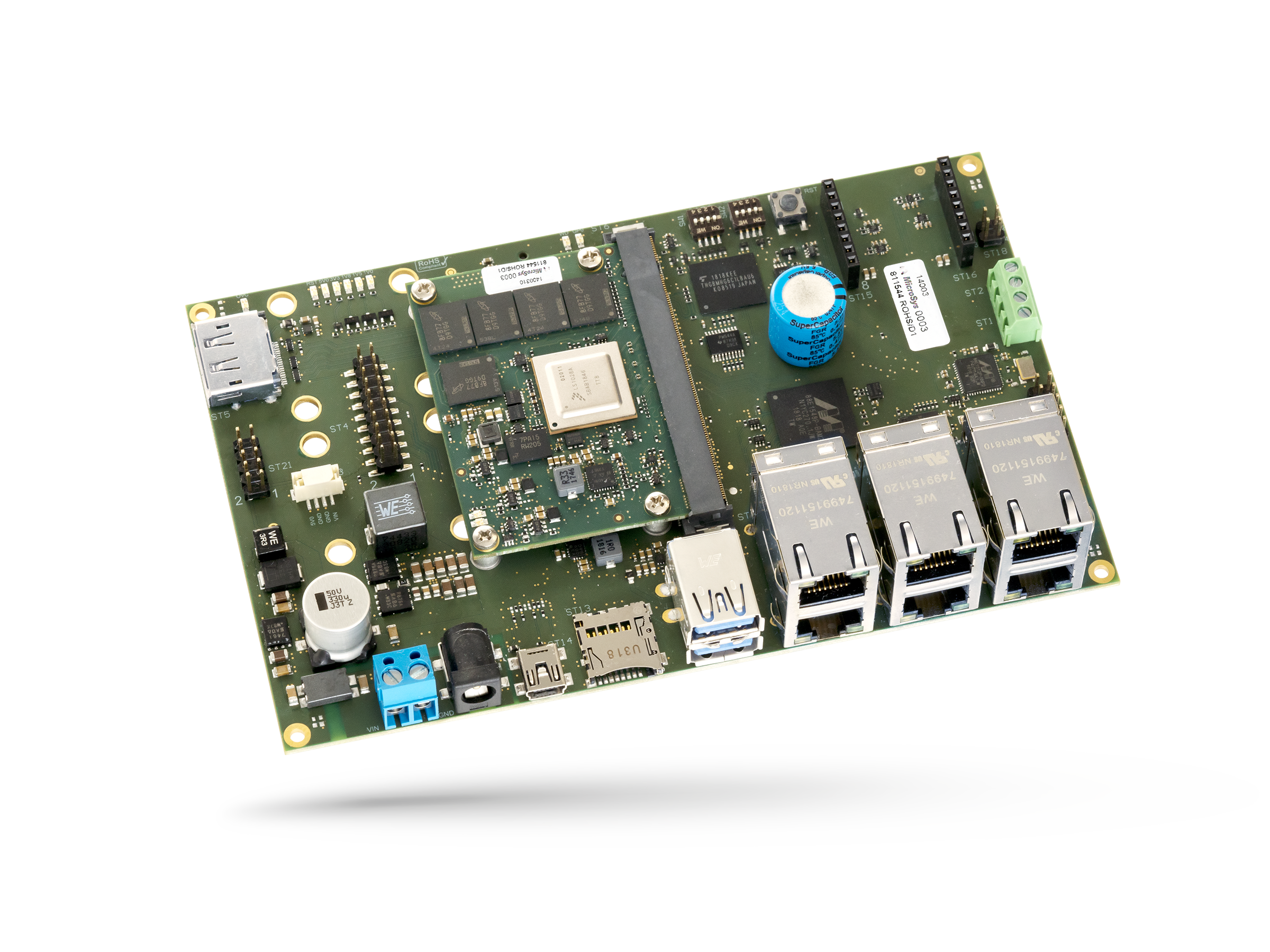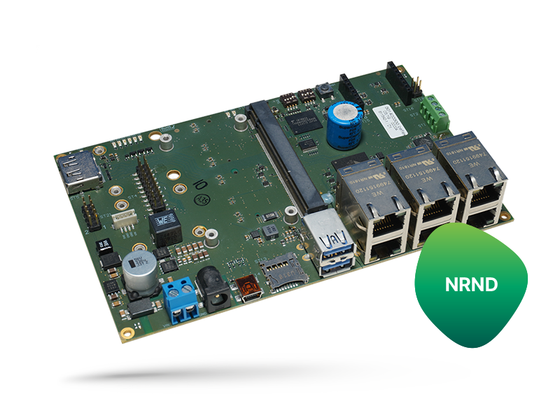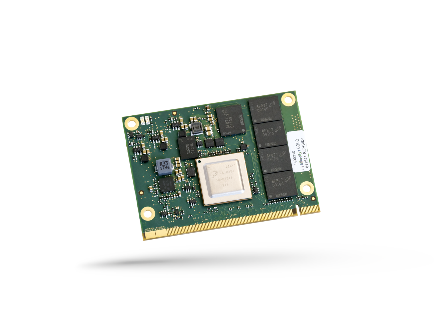


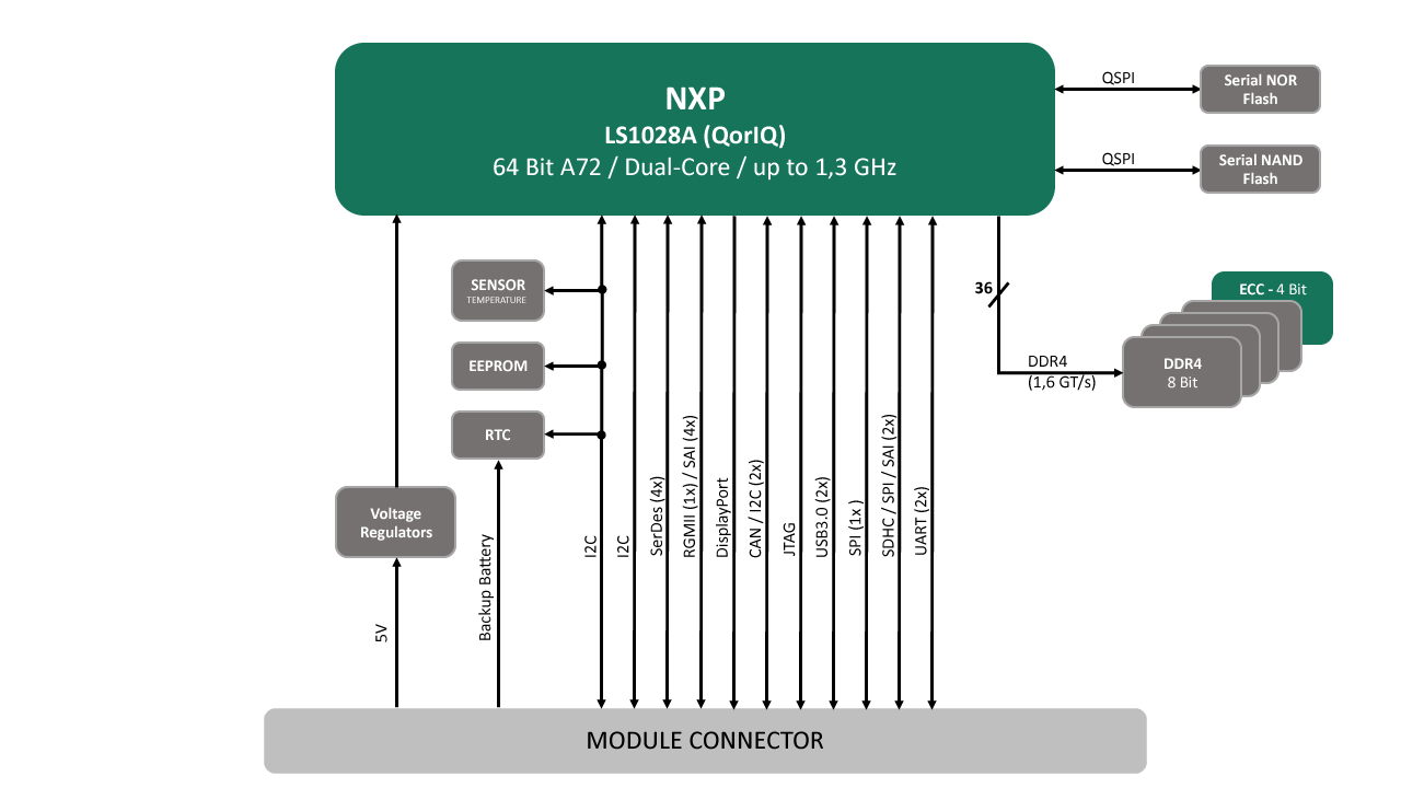
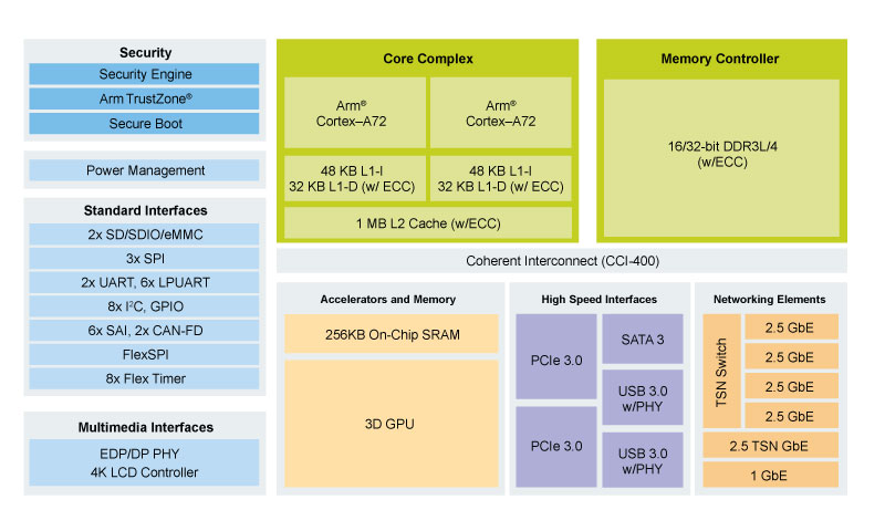
Block Diagrams
Features
| CPU | |
|---|---|
| Architecture | Arm® Cortex®-A72 |
| Processor | NXP® QorIQ® LS1028A CPU: 2 Arm® Cortex®-A72 64-bit cores at up to 1.5 GHz core frequency |
| DRAM | Up to 4 GB 32-bit DDR4 ECC RAM 1600 MT/s |
| Memory | |
| Flash | Up to 256 MB Serial NOR Flash & up to 512 MB Serial NAND Flash |
| Flash Card | 2x SDHC |
| Boot Flash | SDHC, eMMC, XSPI, NAND Flash |
| eMMC | 8-bit |
| EEPROM | Yes |
| Graphic | |
| Graphics Controller | Yes |
| Display | Display Port 1.3 and eDP1.4 |
| Ethernet | |
| 10GbE | 1x SXGMII / QXGMII |
| RGMII | 1x |
| SGMII | 4x 1.25 Gbps |
| QSGMII | 1x 5 Gbps |
| TSN / IEEE 1588 | Yes (4 Port TSN Switch on board) IEEE 802.1 |
| High Speed IO | |
| SerDes lanes | 4x SerDes lanes at 10 Gbps |
| USB 3.0 | 2x |
| PCIe | 4x PCIe Gen3 |
| SATA | 1x GEN3 |
| IO | |
| FlexSPI | 3x |
| UART | 2x |
| CAN FD | 2x |
| I2C | 8x |
| Audio | Yes (SAI) |
| GPIOs | Yes |
| JTAG Debug Interface | Yes |
| Security / Safety | |
| Security | Trust Architecture |
| Operating Condition | |
| Power Supply Voltage | Single 5 V DC input supply voltage range |
| Typical Power Consumption | 5W |
| Power Management | Yes |
| RTC | PCF85063 |
| Temperature | 0 °C to 70 °C |
| Optional Extended Temperature | -40 °C to +85 °C |
| Mechanical | |
| Dimensions | 45 mm x 62 mm |
| Connector Type | 230 pin 0.5 mm pitch |
| Software / Additional | |
| Software Support |
|
| Additional |
Graphics processing unit:
|
Order Info
| Name | Code | Description | Status |
|---|---|---|---|
| miriac® MPX-LS1028A | 857001 | 2 Arm® Cortex®-A72, 1.3 GHz, 4 GB DDR4 w ECC, 16 MB NOR Flash, 512 MB Nand Flash, 0 °C to 70 °C, w SEC | EOL |
| Development Kit basic for miriac® MPX-LS1028A | 8576xx |
|
EOL |
Downloads
FAQ
Q: It is unclear whether the SAI blocks are Slave only or do they support Master mode too?
A: The SAI blocks work in Slave mode only
Q: We expect to configure the SAI in Synchronous mode and each of the peripheral shown has 5 critical signals (Bit Clk, Fsync, Din Dout & Mclk). The SAI blocks however has 7 signals (TX Bit Clk, RX Bit Clk , TX Fsync, RX Fsync, TX Data, RX Data & Mclk). How does the mapping work in this case?
A: SAI Block has 6 signals (TX Bit Clk, RX Bit Clk , TX Fsync, RX Fsync, TX Data, RX Data) and TX signals are multiplexed with Rx signals. Hence only one can be used at a time.This requires that 2 SAI modules are used per CODEC.
Q: For instance TX Data & RX Data are mapped to the same physical pin on the SOC, (SAI4 TX_DATA and RX_DATA mapped to EC1_TXD2) how do I map 2 external signals to a single pin on SOC?
A: Using RCW
Q: In our environment, we need solutions that are available over a very long period of time (up to 15 years). How long are your modules available?
A: Using NXP CPUs on our SoMs we are able to provide an availability of 15 years from the time of the launch of the CPU. With LTB and long-time stocking we are even able to extend this period.
RCW[EC1_SAI4_5_PMUX] = 0b010 – { SAI5_TX_DATA, SAI4_TX_DATA, SAI5_TX_SYNC, SAI4_TX_SYNC, SAI5_TX_BCLK, SAI4_TX_BCLK}
RCW[EC1_SAI4_5_PMUX] = 0b011 – {SAI5_RX_DATA, SAI4_RX_DATA, SAI5_RX_SYNC, SAI4_RX_SYNC,SAI5_RX_BCLK, SAI4_RX_BCLK}